GPU architecture
Throughput vs. latency processors
CPUs and GPUs solve the same fundamental problem – executing instructions on data – but they do so with radically different design philosophies. Figure 1 illustrates the key structural difference.
After working through this lecture, you should be able to:
- explain the difference between latency-optimized (CPU) and throughput-optimized (GPU) processor design,
- describe the GPU execution model: kernels, threads, warps/wavefronts, thread blocks and SMs/CUs,
- navigate the GPU memory hierarchy (registers, shared memory, caches, global memory),
- define occupancy, compute it for a given kernel resource usage, and explain its role in latency hiding,
- translate between NVIDIA, AMD and Intel terminology for the same hardware concepts.
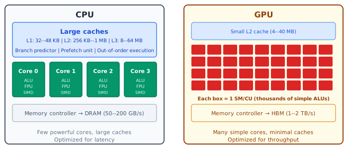
A CPU is a latency-optimized processor. It has a small number of powerful cores (typically 4–128), each with deep pipelines, large caches and sophisticated branch predictors. The goal is to execute a single thread of instructions as fast as possible. When a core stalls waiting for data from memory, the caches and prefetchers work to hide that latency.
A GPU is a throughput-optimized processor. It has a large number of simple cores (thousands), with far less cache per thread and no branch prediction. The goal is to keep as many threads running as possible. When a group of threads stalls waiting for data, the hardware switches to another group that is ready to execute. Latency is hidden not by caches but by massive parallelism.
This leads to a key design constraint:
GPU code must expose enough parallelism – typically tens of thousands of independent threads – so that the hardware always has work to switch to while waiting for memory.
The following table summarizes the differences:
| CPU | GPU | |
|---|---|---|
| Cores | Few (4–128), complex | Many (thousands), simple |
| Threads | Few per core (1–2 via SMT) | Many per core (hundreds active) |
| Caches | Large, automatic | Small, programmer-managed |
| Latency hiding | Caches + prefetching | Thread switching |
| Optimal workload | Complex, branchy, serial | Simple, uniform, massively parallel |
The GPU execution model
Threads, warps and thread blocks
A kernel is a function that is compiled for the GPU and launched from the host: it is instantiated once per thread, and every thread executes the same kernel code on different data. GPU programs launch a large number of threads this way. This model is known as SIMT (Single Instruction, Multiple Threads).
Threads are organized into a two-level hierarchy:
Thread blocks (or workgroups): a group of threads that execute on the same processing unit and can cooperate through fast shared memory and synchronization barriers.
Grid: the collection of all thread blocks launched by a single kernel. Blocks in a grid are independent and can execute in any order.
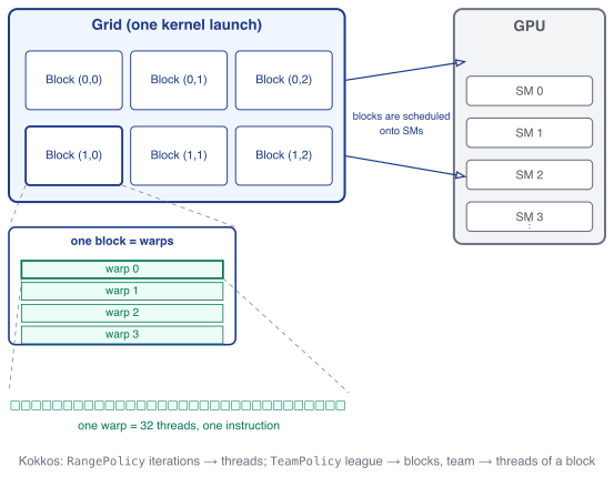
Within a thread block, threads are further grouped into warps (NVIDIA) or wavefronts (AMD). A warp/wavefront is the smallest unit of scheduling: all threads in a warp execute the same instruction at the same time on different data. Figure 2 shows how the levels nest and how they map onto the hardware.
The warp/wavefront size is a fundamental hardware parameter:
- NVIDIA GPUs: warp size = 32 threads
- AMD GPUs: wavefront size = 64 threads (some RDNA GPUs support 32)
Streaming multiprocessors and compute units
The physical execution units on a GPU are called Streaming Multiprocessors (SMs) on NVIDIA hardware and Compute Units (CUs) on AMD hardware. Each SM/CU can execute multiple warps/wavefronts concurrently and contains:
- A set of arithmetic units (INT, FP32, FP64, tensor cores)
- A register file (shared among all active threads)
- Shared memory (fast, on-chip scratchpad)
- Warp/wavefront schedulers
A typical modern GPU has 50–150 SMs/CUs. When a kernel launches, the GPU’s hardware scheduler distributes thread blocks across the available SMs/CUs, as sketched on the right of Figure 2.
Once a block is assigned to an SM, it runs to completion on that SM. Multiple blocks can be assigned to the same SM if there are enough resources (registers, shared memory). The hardware handles scheduling automatically; the programmer controls only the block size and the total number of blocks.
SIMT execution and warp divergence
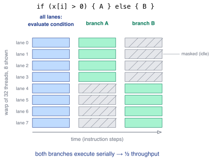
Within a warp, all 32 (or 64) threads execute the same instruction simultaneously. This works perfectly when all threads take the same path through the code. But what happens with conditional branches? Consider a kernel where even-numbered threads call function A and odd-numbered threads call function B. Since all threads in a warp must execute the same instruction, the hardware handles this by executing both branches sequentially while masking the threads that should not participate:
- Execute function A for even threads; odd threads are idle.
- Execute function B for odd threads; even threads are idle.
This is called warp divergence (or branch divergence); Figure 3 illustrates the serialization. In the worst case (half the warp goes each way), throughput is halved. Warp divergence is one of the most common performance pitfalls in GPU programming.
Structure your code so that threads within the same warp take the same branch. For example, if you must branch, make the condition depend on the block index rather than the thread index – then entire warps go one way or the other, with no divergence within a warp.
GPU memory architecture
The memory hierarchy
GPUs have a memory hierarchy similar in concept to CPUs, but different in character (Figure 4). From fastest to slowest:
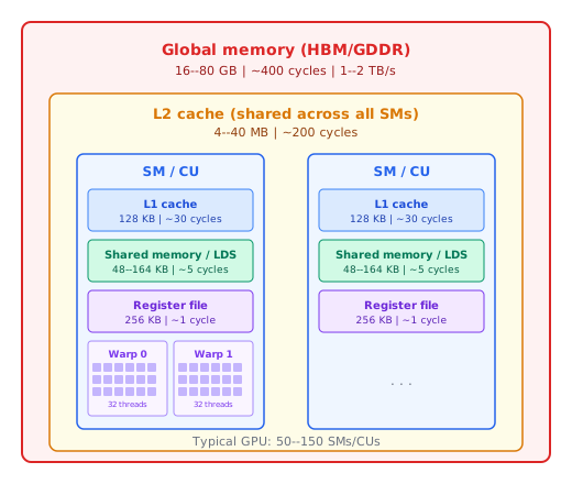
  Per-thread    Registers          ~1 cycle       Fastest, most limited
      ↓
  Per-block     Shared memory      ~5 cycles      Programmer-managed scratchpad
      ↓
  Per-SM        L1 cache           ~30 cycles     Automatic (configurable on some GPUs)
      ↓
  Per-GPU       L2 cache           ~200 cycles    Automatic, shared across all SMs
      ↓
  Per-GPU       Global memory      ~400 cycles    Largest, slowest (HBM or GDDR)
The key differences from a CPU memory hierarchy:
- Registers are abundant (tens of thousands per SM) but shared among all threads on the SM. More registers per thread means fewer threads can be active simultaneously.
- Shared memory is a fast, programmer-managed scratchpad within a block. Unlike a CPU cache, the programmer explicitly loads data into shared memory and reads it back. It is called Local Data Share (LDS) on AMD GPUs.
- L1 and L2 caches exist on modern GPUs but are much smaller relative to the data being processed. The primary latency-hiding mechanism remains thread switching, not caching.
- Global memory is the main GPU memory (HBM2/HBM3 on data center GPUs, GDDR6 on consumer GPUs). It is large (16–80 GB on current hardware) but has high latency. Efficient access requires memory coalescing, discussed in detail in the memory performance lecture.
Registers
Each thread has its own private set of registers. Registers are the fastest storage on the GPU (~1 cycle access), but they are a finite resource shared across all active threads on an SM. A typical SM has 65,536 32-bit registers.
If a kernel uses 32 registers per thread and the SM has 65,536 registers, then at most \(65{,}536 / 32 = 2{,}048\) threads can be active on that SM simultaneously. If the kernel uses 64 registers per thread, only 1,024 threads can be active – reducing the GPU’s ability to hide latency by switching between threads.
When a kernel needs more registers than the hardware provides, the compiler spills excess register values to slow global memory. Register spilling is a major performance concern and can be diagnosed with profiling tools.
Constant and texture memory
Older GPU programming guides emphasize constant memory (read-only, cached, 64 KB on NVIDIA) and texture memory (cached with spatial locality optimizations). On modern GPUs (Volta and later on NVIDIA, RDNA on AMD) the unified L1/L2 caches have largely subsumed these special memory types. They still exist for backward compatibility but are rarely essential for new code.
Latency hiding and occupancy
The GPU’s core trick: latency hiding
CPUs invest transistors in caches and branch predictors to reduce the effective latency of each memory access. GPUs take a fundamentally different approach: they accept high latency but keep enough threads in flight that there is always a warp ready to execute while others wait for data.
Consider a simplified example. A warp issues a global memory load that takes 400 cycles. If the SM has only one warp, it sits idle for 400 cycles. But if the SM has 20 warps, it can cycle through the other 19 while waiting – executing 20 useful instructions per cycle instead of 1 every 400 cycles. Figure 5 contrasts the two situations.
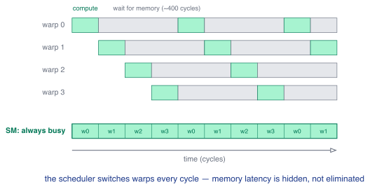
This is why GPUs need massive parallelism: the more warps that are active, the more effectively memory latency is hidden.
Occupancy
Occupancy is the ratio of active warps on an SM to the maximum number of warps the SM supports:
\[\text{Occupancy} = \frac{\text{active warps per SM}}{\text{max warps per SM}}\]
For example, an NVIDIA A100 SM supports up to 64 active warps (2,048 threads). If your kernel configuration results in 32 active warps per SM, the occupancy is 50%.
Occupancy is limited by three resources:
- Registers per thread: more registers per thread → fewer threads fit on the SM.
- Shared memory per block: more shared memory per block → fewer blocks fit on the SM.
- Threads per block: if the block size does not evenly divide the SM’s capacity, some slots go unused.
Worked example. Suppose a kernel uses 48 registers per thread on an SM with 65,536 registers and a maximum of 2,048 threads (64 warps). The register file then accommodates at most \(\lfloor 65{,}536 / 48 \rfloor = 1{,}365\) threads. Since threads are scheduled in warps of 32, this rounds down to \(\lfloor 1{,}365/32 \rfloor = 42\) active warps, i.e. 1,344 threads. The occupancy is therefore \(42/64 \approx 66\%\) – the kernel is register-limited: it cannot reach full occupancy no matter how the block size is chosen. Reducing register usage to 32 per thread would allow all 2,048 threads (100% occupancy).
Higher occupancy generally means better latency hiding, but it is not always the most important metric. A kernel that achieves 50% occupancy but makes excellent use of registers and shared memory can outperform a kernel at 100% occupancy that constantly accesses global memory. The goal is sufficient occupancy to hide latency, not maximum occupancy at any cost.
A good starting point is to aim for at least 50% occupancy. Use profiling tools (ncu for NVIDIA, rocprof for AMD) to measure actual occupancy and identify whether register usage or shared memory is the limiting factor.
Vendor nomenclature
The three major GPU vendors use different terminology for the same concepts. The following table provides a mapping:
| Concept | CUDA (NVIDIA) | ROCm/HIP (AMD) | SYCL/oneAPI (Intel) |
|---|---|---|---|
| Thread | Thread | Thread / Work-item | Work-item |
| Scheduling unit | Warp (32) | Wavefront (64) | Sub-group (8–32) |
| Thread group | Thread block | Workgroup | Work-group |
| Processing unit | Streaming Multiprocessor (SM) | Compute Unit (CU) | Execution Unit (EU) |
| All thread groups | Grid | Grid | ND-range |
| Fast on-chip memory | Shared memory | LDS (Local Data Share) | SLM (Shared Local Memory) |
| Kernel launch | <<<blocks, threads>>> |
hipLaunchKernelGGL |
queue.submit |
| Compiler | nvcc |
hipcc / amdclang++ |
icpx -fsycl |
Note that Intel’s terminology has shifted: what older oneAPI documentation calls an Execution Unit (EU) is now referred to as a vector engine, several of which are grouped into an Xe-core on current Intel GPU architectures.
The Kokkos hardware abstraction layer provides a portable interface over these vendor-specific models. It maps thread blocks to teams, grids to leagues, and shared memory to a scratch memory space, allowing the same C++ code to run on all three platforms.
Outlook: from GPU concepts to the LBM project
The concepts of this lecture map directly onto the Lattice Boltzmann solver you will build in the course project. The natural parallelization is one thread per lattice site: the collision step is purely local and therefore embarrassingly parallel, ideally suited to the SIMT model. The streaming step reads the nine population values from neighboring sites, so each thread performs nine neighbor accesses per update – whether these accesses coalesce into few memory transactions depends entirely on how the populations are laid out in memory. Since the LBM is strongly memory-bound, this layout question dominates performance; it is the subject of the memory performance lecture.